In the fast-evolving world of semiconductor production, precision is crucial. Manufacturers constantly seek methods to enhance efficiency and accuracy. One technology that stands out is laser cutting. But why is laser cutting used in semiconductor production? This question highlights the importance of laser technology in this field.
Laser cutting provides several advantages that traditional methods cannot match. Its ability to create intricate patterns with minimized material waste is unmatched. Additionally, the laser process minimizes the risk of damage to temperature-sensitive materials. This aspect is vital when working with delicate semiconductor components. Moreover, the speed of laser cutting meets the demands of modern production lines.
Experts agree that adopting laser cutting can significantly improve output quality. However, some may overlook its higher initial setup costs. This factor can make new adopters hesitant. Despite the challenges, the benefits of laser cutting in semiconductor manufacturing are undeniable. It plays a pivotal role in ensuring high precision and efficiency in production.
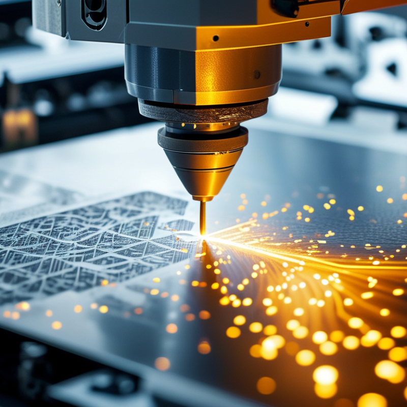
Precision is paramount in semiconductor manufacturing. Laser cutting technology has revolutionized this industry. It delivers unmatched accuracy, which is vital for microfabrication processes. A study by the International Journal of Advanced Manufacturing Technology reported that laser cutting achieved tolerances of less than 10 microns. This level of precision minimizes defects in semiconductors, enhancing product reliability.
Laser cutting also allows for complex geometries. This is essential as devices become smaller and more intricate. Traditional methods often struggle with such demands. With laser technology, manufacturers can produce intricate patterns without compromising on quality. However, not all laser systems are created equal. Choosing the right type of laser, based on the semiconductor material, can be crucial.
Tip: Always validate the laser options with material compatibility. Testing different settings can yield better results.
Another consideration is the heat-affected zone (HAZ). Laser cutting can create unwanted thermal effects on materials. This can lead to warping or changes in electrical conduction. It is essential to optimize laser parameters to mitigate these issues. Regular monitoring and adjustments can enhance precision while maintaining structural integrity.
Tip: Implement routine checks to assess laser performance. Small adjustments can prevent significant errors.
Laser cutting technology plays a crucial role in semiconductor manufacturing due to its ability to provide high precision, increased speed, versatility with different materials, reduction of waste, and overall cost efficiency. These factors significantly enhance the production processes in the semiconductor industry.
Laser cutting has transformed semiconductor production by enhancing material efficiency significantly. This technique utilizes high-powered lasers to precisely cut various materials with minimal waste.
The accuracy of laser cutting reduces the amount of scrap produced during the fabrication process. This precision is crucial in semiconductor manufacturing, where even small imperfections can lead to functional failures.
The adaptability of laser cutting to different materials is another advantage. It can handle both metal and non-metal substrates. This versatility allows manufacturers to optimize their processes based on specific project needs. However, not all materials respond equally to laser cutting. Some require adjustments in settings to prevent distortion or damage. This aspect necessitates careful planning and expertise.
Incorporating laser cutting into production workflows also poses challenges. Technicians need to be skilled in operating laser technologies and understanding their limitations. Even slight miscalculations can impact the overall efficiency of operations. Hence, continuous training and development are essential in this field. Balancing efficiency and accuracy is key to harnessing the full potential of laser cutting in semiconductor production.
Laser cutting plays a crucial role in semiconductor production. Its efficiency can significantly minimize production time and costs. Unlike traditional methods, laser cutting provides precision and speed that boost productivity. This ability to cut intricate designs allows manufacturers to optimize material usage, creating less waste and saving money.
Tips: Always assess the specific cutting requirements for each project. This avoids unnecessary adjustments and delays. Understanding the thickness and type of material is important for optimal results.
Utilizing advanced laser cutting technologies can enhance the overall quality of semiconductor products. However, it’s essential to ensure that operators are adequately trained. Poor handling can lead to defects, undermining the benefits of laser cutting. Regular maintenance of laser equipment is also critical. This prevents downtime, which can hinder production timelines and increase costs.
Incorporating laser cutting into your production process requires careful planning. Striking a balance between speed and precision is necessary. It’s important to focus on developing effective workflow strategies. Ultimately, the goal is to streamline production while maintaining high-quality standards.
| Reason | Description | Benefits | Impact on Production |
|---|---|---|---|
| Precision | Laser cutting achieves high accuracy and minimal kerf width. | Improves product quality and reduces material wastage. | Accelerates the prototyping and manufacturing processes. |
| Versatility | Can cut through a variety of materials including silicon and metals. | Adapts to different applications in semiconductor fabrication. | Reduces the need for multiple machines, thus streamlining operations. |
| Speed | Laser cutting can perform tasks much faster than traditional methods. | Shorter turnaround times enhance efficiency. | Increases overall throughput of semiconductor production lines. |
| Automation | Easily integrates with automated systems for mass production. | Reduces labor costs and human error. | Enhances reliability and consistency in output. |
| Cost-Effectiveness | Lower operational costs due to reduced waste and faster processes. | Saves money on materials and production time. | Improves ROI for semiconductor manufacturing investments. |
Laser cutting stands out as a critical technology in semiconductor production, streamlining intricate designs with remarkable precision. According to a report from MarketsandMarkets, the laser cutting market in semiconductors is projected to grow at a compound annual growth rate of 7.5% from 2022 to 2027. This growth underlines the increased reliance on laser cutting for optimizing production efficiency and design complexity.
The versatility of laser cutting methods allows for the fabrication of detailed components. These methods can handle various materials, from silicon wafers to advanced composite substrates. Laser cutting not only provides accuracy but also reduces material waste compared to traditional cutting methods. However, the technology is not without challenges. Variations in substrate thickness may lead to inconsistent cuts, indicating that operators need refined skills to minimize errors.
Achieving complex designs demands high precision, which can sometimes result in longer processing times. High initial costs can deter smaller manufacturers from adopting this technology, despite its long-term benefits. Continuous training and investment in equipment maintenance are vital to maintaining optimal performance levels. The trade-offs in adopting laser cutting technology reveal both opportunities and obstacles, prompting manufacturers to weigh their options carefully.
Laser cutting has become a cornerstone in semiconductor production. It provides unmatched precision, ensuring that components meet strict standards. Manufacturers rely on laser technology to achieve intricate designs with minimal waste. This capability is crucial as even the slightest defect can result in significant performance issues.
Consistency is another key benefit of laser cutting. Each cut is reproducible, which is critical in high-volume semiconductor manufacturing. This method allows for uniformity across all components, reducing the variability that can occur with traditional cutting methods. However, achieving perfect consistency is challenging. Even minor variations in the laser settings can lead to discrepancies.
Quality assurance is integral to the semiconductor industry. Laser cutting enables detailed inspection and adjustments during production. This technology helps identify flaws early, before they escalate into costly problems. Yet, some processes may still need manual oversight for complex designs. Balancing automation with human insight remains a necessary consideration.
: Precision ensures high quality and reliability in semiconductors, minimizing defects and enhancing product performance.
Laser cutting allows for unmatched accuracy, enabling intricate designs with minimal material waste compared to traditional methods.
HAZ refers to thermal effects that can warp materials, impacting their electrical properties. Proper adjustment in laser settings helps mitigate this.
No, different materials require specific laser types and settings. Validation for compatibility is crucial to achieve desired results.
Technicians must understand laser operation and its limitations. Miscalculations can significantly impact production efficiency.
Implementing regular performance checks and continuous training for staff helps maintain precision and reduces errors in production.
Laser cutting reduces scrap material and allows complex designs, but it requires skilled operators for optimal results.
Different materials may respond uniquely to laser cutting, necessitating careful planning to avoid distortion or damage during cutting.
High initial costs can deter smaller manufacturers, but the long-term efficiency benefits can justify the investment.
Yes, it can cut both metal and non-metal substrates, but adjustments may be necessary based on specific material characteristics.
Laser cutting plays a pivotal role in semiconductor production for several reasons. Firstly, precision is paramount in this field, and laser cutting offers unparalleled accuracy, ensuring that each component meets stringent specifications. This precision is essential for the integrity and functionality of semiconductor devices. Additionally, laser cutting enhances material efficiency, allowing manufacturers to minimize waste and optimize resource use.
Further, the quick turnaround provided by laser cutting techniques significantly reduces production time and costs, making it a preferred choice in the industry. The versatility of these methods also enables the creation of complex designs that are increasingly required in modern semiconductors. Lastly, consistency and quality in semiconductor components are upheld through the use of laser cutting, ensuring reliable performance. Thus, understanding why is laser cutting used in semiconductor production highlights its indispensable contributions to manufacturing efficiency and product excellence.
Stylo Laser