A clean PCB cut is more than a straight line. It protects copper traces, keeps board edges consistent, and helps components fit during assembly. A small deviation can leave a rough edge or bring a cutter too close to a conductor. The damage may be easy to miss at first. Later, it can cause fitting problems or require a replacement board.
So, why is precision important in PCB cutting? It affects both product quality and production efficiency. Accurate cutting helps maintain the board’s specified dimensions and reduces unnecessary material waste. It also supports repeatable results across multiple panels. In practice, precision depends on several factors: the cutting method, tool condition, board material, machine setup, and operator checks. Even a well-calibrated machine can produce poor results if a worn bit or loose fixture shifts the panel.
There is no single setting that works for every board. Thin substrates, dense layouts, and different laminate types may respond differently to cutting. That part is sometimes underestimated. A practical process starts with checking the design clearance, securing the panel, and selecting a suitable tool and feed rate. Operators should inspect cut edges and measure sample boards, rather than trusting machine settings alone. Small checks matter. Still, measurement records can be incomplete, and a visually neat edge does not prove that every dimension is correct. This guide explains ways to improve PCB cutting precision and why those improvements matter, while recognizing that real production conditions can complicate even a careful process.
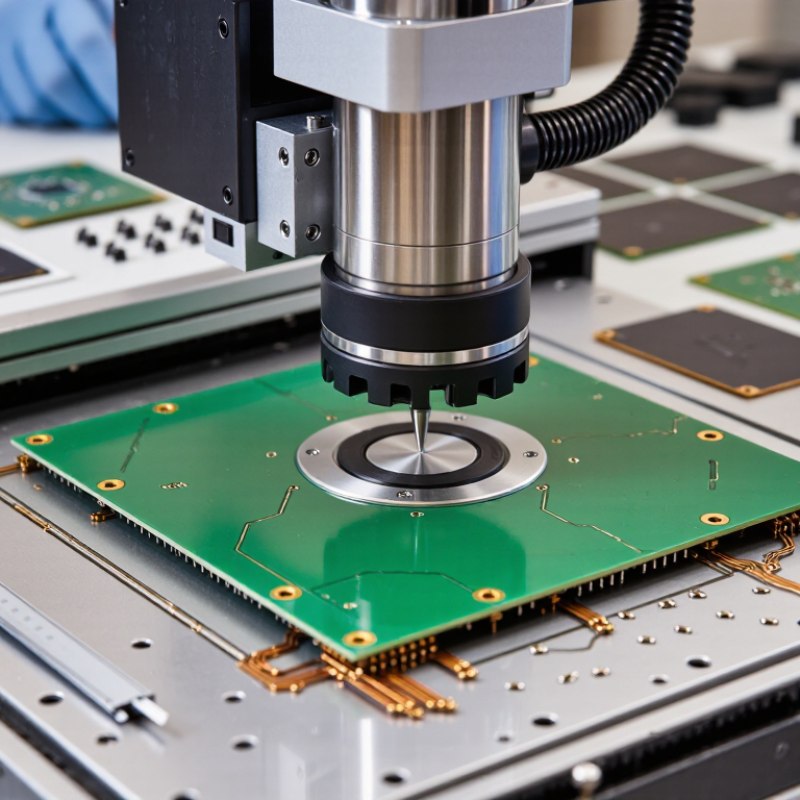
Understanding PCB Cutting Precision and Its Role in Board Quality
PCB cutting precision is the accuracy with which a board’s outline and edges match the design dimensions. It affects more than appearance. A small routing error can leave a board too wide for its enclosure or shift connector openings away from their intended positions. That mismatch can complicate assembly and put stress on nearby components. Clean, consistent edges also reduce burrs and splintering, which may interfere with handling or inspection. Details matter.
Precision depends on the cutting method, tool condition, board material, and how securely the panel is held. For example, a worn cutter may produce rough edges, while vibration can cause the outline to wander. Checking dimensions against the design and inspecting sample edges under good lighting can reveal issues early. One measurement is not enough. I have seen teams focus on the machine settings and overlook how a loose fixture affects repeatability; that is an easy assumption to revisit.
Tips: Secure the panel before cutting, replace dull tools, and measure several boards from different positions. Record edge quality as well as dimensions. If results vary, pause and check the fixture, cutter, and material support before changing multiple settings at once. Small checks help. Be realistic, though: tighter tolerances may require more time and careful process control, and not every board needs the same level of precision.
How to Improve PCB Cutting Precision and Why It Matters?
Selecting the Right Tools and Parameters for Accurate PCB Cutting
Accurate PCB cutting starts with a tool suited to the board’s material and thickness. A sharp, rigid cutting bit helps reduce edge burrs and unwanted vibration. For repeated production, a CNC router can follow a defined path more consistently than freehand cutting. Check that the worktable supports the board evenly. Even slight movement can shift a cut by a fraction of a millimeter.
Set spindle speed, feed rate, and cutting depth as a working combination, not isolated numbers. A feed rate that is too high may pull at copper or leave rough edges. Too slow, and heat can build up around the cut. Test settings on a scrap section from the same panel. Measure the finished edge with calipers, then inspect it under magnification. Small details matter. Keep dust extraction clear, and replace dull bits promptly.
Secure the panel with clamps or a suitable vacuum fixture, while avoiding pressure that bends thin boards. Leave enough clearance around traces and components, and confirm the toolpath before cutting. I have found that a clean-looking edge does not always mean the board is undamaged; hidden delamination can be easy to miss. There is room for judgment here. Record successful settings for each board thickness, but verify them again when the material or tool changes.
Calculated chip load per tooth at a constant spindle speed of 30,000 rpm using a 2-flute cutter.
Chip load is calculated as feed rate ÷ (spindle speed × number of flutes). At 30,000 rpm with two flutes, increasing feed rate from 100 to 500 mm/min raises chip load from about 1.67 to 8.33 μm per tooth. Use machine, cutter, and material specifications to choose suitable settings; this chart illustrates the calculation, not a universal cutting recommendation.
Before cutting, inspect the bare PCB under bright, angled light. Look for chipped edges, copper burrs, moisture marks, and panels that rock on a flat surface. IPC-1601A, the industry’s printed-board handling guideline, stresses controlling moisture exposure because absorbed moisture can contribute to delamination during later heating. Keep boards sealed until use, then allow them to reach room temperature before machining. A cold panel moved into a warm shop can collect condensation. Easy to miss.
Clean the cutting bed and check that its vacuum holds the panel firmly across the full work area. Even slight movement can widen a routed slot or leave a rough edge. Verify the cutter’s runout, tool wear, spindle speed, and feed rate against the tool and board manufacturer’s technical data. Use a scrap coupon to test the setup; measure the cut with calibrated calipers, and compare it with the drawing tolerance. NIST’s measurement guidance highlights the importance of accounting for measurement uncertainty, so avoid treating one caliper reading as absolute truth.
Tips: Record panel thickness, room temperature, tool changes, and test-cut measurements for each setup. A simple log often reveals drift before it becomes a batch problem. Replace a dull bit early; waiting for visible damage is not a great inspection method.
| Preparation Area | Recommended Check or Action | Why It Matters | Practical Acceptance Check |
|---|---|---|---|
| PCB material condition | Inspect panels for warping, cracks, delamination, and damaged edges before cutting. | Defects or uneven surfaces can shift the cutting path and increase the risk of breakage. | Panel lies flat on the support surface and has no visible damage in the cutting area. |
| Material identification | Confirm the board type, thickness, layer structure, and required cut dimensions against the job documentation. | Different materials and thicknesses may require different tooling, feed settings, and support arrangements. | Recorded material details match the work order and the approved drawing. |
| Moisture and storage | Follow the material supplier’s storage and conditioning guidance; keep boards clean and dry before processing. | Moisture and contamination can contribute to dimensional changes, poor edge quality, or handling problems. | No condensation, dust, or visible residue is present on the panel. |
| Machine cleanliness | Remove dust and debris from the work surface, clamps, guides, and material-contact areas. | Particles beneath a panel can cause rocking or uneven positioning, reducing cut accuracy. | Contact surfaces are clean, unobstructed, and free of loose debris. |
| Tool condition | Check the cutting tool for wear, chips, damage, and secure installation; replace it when it no longer meets process requirements. | A worn or damaged tool can produce rough edges, excess heat, dimensional variation, or tool breakage. | Tool condition is acceptable under the site’s inspection criteria and the tool is firmly secured. |
| Workholding and support | Position clamps and supports so the board is held securely without obstructing the cutting path or damaging the panel. | Movement or vibration during cutting can cause inaccurate dimensions and inconsistent edges. | Panel remains stable during a dry run and is supported near the cutting area as required. |
| Alignment and registration | Verify panel orientation, datum points, stops, and programmed coordinates before starting the cut. | Incorrect registration can shift cuts relative to board features and reduce usable panel area. | Reference points and cut path agree with the approved setup drawing. |
| Machine settings | Confirm the selected program, feed rate, spindle or blade settings, and depth against the validated process for the material. | Unsuitable settings may increase tool load, heat, vibration, or edge defects. | Settings are documented and verified before production; changes are controlled. |
| Calibration and maintenance | Check that relevant axes, stops, and measuring devices are within the machine’s scheduled calibration and maintenance requirements. | Calibration drift or mechanical play can create repeatable dimensional errors. | Inspection and maintenance records are current, with no unresolved accuracy issues. |
| Trial cut and first-piece inspection | Where appropriate, make a trial cut and measure the first completed piece before continuing with the batch. | Early verification can reveal setup errors before they affect multiple boards. | Critical dimensions and edge condition meet the drawing and applicable acceptance criteria. |
| Dust extraction and operator safety | Confirm extraction, guarding, emergency stops, and required personal protective equipment are in place. | PCB cutting can generate dust and mechanical hazards; safe operation also helps maintain a clean work area. | Safety devices function correctly and extraction is operating before cutting begins. |
Improving PCB cutting precision starts before the tool touches the board. Check that the panel is flat and firmly supported, with no debris beneath it. Even a thin chip can tilt the workpiece. Secure the board without bending it, then confirm that the cutting path matches the intended outline. Measure a test cut on scrap material and inspect the edge under bright light. Small shifts matter. If the edge shows tearing or copper burrs, review the tool condition and feed settings rather than compensating by eye.
Change one setting at a time. A slower feed may improve control, but excessive heat can soften the substrate and leave a rough edge. Keep the cutter sharp, use consistent clamping pressure, and avoid forcing the tool through corners. Pause to clear dust when it obscures the cut line. After cutting, compare key dimensions with a caliper and check that nearby traces remain undamaged. Record the material, tool condition, and settings so repeat jobs start from evidence, not memory. In practice, I would still recheck the first board from each new panel; identical-looking sheets do not always cut identically. That extra check takes time, and it can feel unnecessary. It has also caught small alignment errors that were easy to miss.
PCB cutting precision is best judged with repeatable measurements, not appearance alone. A clean-looking edge can still hide uneven width or slight registration drift. Start with a test coupon and record the cut width, edge deviation, and burr size at fixed points. Use the same measuring tools and locations each time. Small shifts matter.
Keep a simple log after each production run. Note the panel material, thickness, cutting speed, tool condition, and measured results. A microscope can reveal fraying that calipers miss, while calipers provide useful width checks. Compare results across several runs, since one unusually good panel proves little. Not every day.
When measurements begin to drift, inspect the cutter and confirm the panel is secured evenly. Change one setting at a time, then cut another coupon and compare it with the baseline. This makes cause and effect easier to see. Still, logs are not perfect: operator pressure or worn measuring tools can skew readings. Record uncertainty, replace questionable tools, and review trends rather than reacting to every small variation. Over time, that routine helps distinguish normal variation from a process that needs attention.
It means the board outline and edges match the planned dimensions. A small error can shift connector openings or prevent enclosure fit. Details matter.
Clean edges reduce burrs, splinters, and handling problems. Rough edges may interfere with inspection or stress nearby components during assembly. Not always obvious.
Tool wear, vibration, loose fixtures, material differences, and incorrect machine settings can affect results. A worn cutter may create rough edges and a drifting outline. The fixture is easy to overlook.
Inspect panels under bright, angled light. Check for chipped edges, copper burrs, moisture marks, and rocking panels. Keep sealed boards at room temperature before machining. Condensation can appear unexpectedly.
Absorbed moisture may contribute to separation between board layers during later heating. A cold panel entering a warm room can collect condensation. That small detail matters.
Clean the cutting bed and confirm the vacuum holds the panel across the work area. Check cutter runout, tool wear, spindle speed, and feed rate. Even slight movement can widen a routed slot.
Use a scrap coupon before production cutting. Measure the result with calibrated calipers and compare it with the drawing tolerance. One reading can mislead. Repeat measurements when possible.
Record panel thickness, room temperature, tool changes, fixture condition, and test-cut measurements. Measure boards from different panel positions. Log edge quality as well as dimensions. A simple log can reveal drift.
Pause before changing several settings at once. Check the fixture, cutter, material support, and machine condition separately. Tighter tolerances require more time and control. Not every board needs extreme precision.
PCB cutting precision plays a direct role in board quality, affecting dimensions, edge smoothness, component spacing, and the reliability of later assembly. Understanding why is precision important in PCB cutting helps manufacturers recognize that even small errors can lead to misaligned features, damaged board edges, or unnecessary material waste. Accurate results begin with choosing suitable cutting tools and setting parameters such as speed, feed rate, and cutting depth to match the board material and thickness.
Preparation is equally important: inspect and secure the PCB, check that the machine is clean and properly calibrated, and confirm the cutting path before starting. During cutting, use a consistent process, avoid excessive force, and monitor for vibration or heat that could cause defects. Afterward, measure the finished board and review any deviations. Recording results and adjusting tools or settings over time can reduce recurring errors and support more consistent PCB production.

Stylo Laser