Why are micro laser systems used in electronics? The answer begins with control. These compact light sources deliver precise energy to tiny areas. In semiconductor fabrication, engineers use them for marking, trimming, drilling, soldering, and inspecting delicate components. A focused beam can create clean features without touching the surface. This matters when circuit boards contain narrow traces, fragile sensors, or heat-sensitive materials. The spot may be only a few micrometres wide. The effect stays local.
Manufacturers also value speed, repeatability, and digital control. A micro laser system can follow programmed paths and adjust pulse duration. It can also record process data for quality checks. In a production room, this may create consistent markings on hundreds of connectors. It can reduce mechanical wear and limit tool changes. Engineers select wavelength, power, pulse width, and cooling for each material. Metals, polymers, ceramics, and silicon respond differently. Practical testing remains essential. A specification sheet cannot predict every reflection, surface defect, or heat-affected zone. Experienced technicians inspect results under magnification and revise settings carefully. The technology is powerful, but not automatically perfect. Poor calibration may cause discoloration, cracking, or hidden electrical damage. Safety enclosures, ventilation, interlocks, and trained operators are part of responsible use. This introduction explores the evidence behind why are micro laser systems used in electronics, while recognizing their costs, limitations, and continuing improvements.
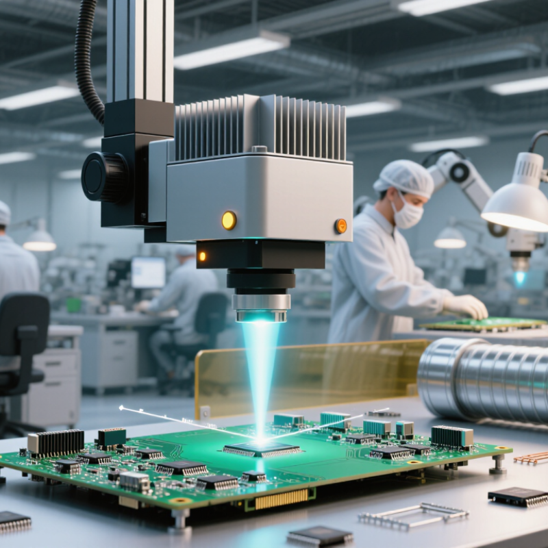
Micro laser systems are compact devices that generate and control highly focused light. In electronics, they usually combine a laser diode, miniature lenses, a driver, and thermal management parts. Some models also include sensors for power and beam-position control. The complete unit may fit inside a handheld tool or a precision manufacturing head.
Their narrow beam can work on tiny electronic features with limited heat spread. Engineers use these systems for circuit inspection, component marking, micro-welding, and selective material removal. A beam can trace a fine line across a circuit board without touching nearby components. During inspection, reflected light may reveal a cracked surface or uneven connection. This level of control supports repeatable results, especially when traditional mechanical tools feel too large.
However, small does not mean simple. Dust on a lens can change the beam profile. Poor calibration may leave a dark mark or damage a thin coating. Heat also matters, even when the visible spot looks tiny. A practical setup needs shielding, stable mounting, verified power settings, and regular optical checks. It is easy to overestimate precision from appearance alone. I would also question whether every task needs a laser; some delicate jobs may still require contact tools or camera-guided inspection. Micro laser systems are useful because they combine focused energy, compact hardware, and measurable control, but their performance depends heavily on setup quality.
| Data Dimension | Typical Characteristics | Relevance to Electronics Manufacturing |
|---|---|---|
| Definition | Computer-controlled laser systems designed to process features that are typically measured in micrometres. | They provide focused, programmable energy for precise cutting, drilling, marking, trimming, welding, and surface treatment of small electronic components. |
| Common Wavelengths | Ultraviolet: approximately 355 nm; visible green: approximately 532 nm; near-infrared: approximately 1,064 nm. | Different wavelengths are absorbed differently by metals, polymers, ceramics, glass, and semiconductor materials, allowing the process to be matched to the workpiece. |
| Pulse Duration | Nanosecond pulses are widely used; picosecond and femtosecond pulses are used when very low thermal damage is required. | Short pulses can remove material rapidly while limiting heat diffusion, which helps protect nearby circuits and delicate insulating layers. |
| Focused Spot Size | Common process spots range from roughly 1 to 50 micrometres, depending on wavelength, optics, pulse characteristics, and material. | A small spot enables fine features, narrow kerfs, closely spaced patterns, and high-density circuit processing. |
| Positioning Precision | High-end motion and galvo systems can provide micrometre-level positioning, although actual accuracy depends on calibration and machine design. | Precise positioning supports reliable processing of microvias, bond pads, conductive tracks, sensors, and miniature connectors. |
| Materials Processed | Copper, aluminum, nickel, stainless steel, silicon, glass, ceramics, epoxy resins, polyimide, solder materials, and composite circuit substrates. | Laser parameters can be adjusted for both conductive and insulating materials without requiring a separate mechanical tool for every material type. |
| Typical Electronic Applications | Microvia drilling, flexible-circuit cutting, PCB depaneling, component marking, resistor trimming, thin-film patterning, and connector processing. | These operations require small feature sizes, repeatable geometry, and controlled material removal that conventional tools may not achieve efficiently. |
| Non-Contact Processing | The laser beam performs the work without direct mechanical contact between the tool and the component. | Non-contact processing reduces tool wear, minimizes mechanical stress, and helps prevent deformation of thin, fragile, or flexible electronic parts. |
| Heat-Affected Zone | The affected zone can be reduced through shorter pulses, optimized fluence, suitable wavelength selection, and controlled scanning. | Lower thermal impact helps preserve dielectric properties, conductor integrity, dimensional stability, and the performance of nearby components. |
| Process Repeatability | Digital motion control and programmable laser parameters allow the same pattern to be reproduced across many parts. | Repeatability supports consistent production quality, automated inspection, and traceable manufacturing workflows. |
| Production Flexibility | Software-controlled patterns can be changed without manufacturing a dedicated cutting die or mechanical tool. | This is useful for prototypes, product variants, short production runs, and frequent design changes in electronics manufacturing. |
| Process Speed | Speed depends on material, thickness, pulse energy, repetition rate, feature geometry, and required surface quality. | High repetition rates and fast beam scanning can support automated production while maintaining fine feature control. |
| Waste and Cleanliness | Material is removed locally, with fumes and particles commonly managed by extraction and filtration systems. | Localized processing can reduce consumable tooling and material waste, while controlled extraction helps protect components and operators. |
| Key Advantages | Fine resolution, non-contact operation, digital control, low mechanical force, and compatibility with complex geometries. | These advantages make micro laser systems suitable for compact, lightweight, high-density, and increasingly miniaturized electronic devices. |
| Important Limitations | Reflective materials, heat-sensitive polymers, debris generation, optical alignment, and process-development requirements can affect results. | Successful production requires appropriate wavelength selection, beam delivery, fixturing, ventilation, safety controls, and validated process parameters. |
It is a compact device that generates and controls a highly focused light beam. A complete unit may fit inside a handheld tool.
Common parts include a laser diode, miniature lenses, a driver, and thermal management components. Some systems add power or beam-position sensors.
They can drill microvias, cut flexible circuits, trim thin films, and remove wire insulation. They also support marking and inspection.
A focused beam can create tiny holes between copper layers. Some holes measure below 100 micrometers in diameter. The beam avoids physical contact.
Yes. They can weld thin battery tabs and other small connections. The surrounding material may remain relatively cool. Still, heat damage is possible.
Reflected light may reveal cracks, uneven connections, or damaged surfaces. A narrow beam examines small features without touching nearby parts.
Wavelength, pulse duration, focus, power, debris control, and heat management all matter. Dust can change the beam profile. Small errors become visible.
Engineers may need several focus and pulse-energy adjustments. A clean-looking cut can still hide delamination. Appearance alone is not enough.
It needs shielding, stable mounting, verified power settings, and regular optical checks. Lens contamination should be checked carefully. Do not assume the setup is precise.
No. Some tasks may suit contact tools or camera-guided inspection better. The smallest beam is not automatically the best solution. That deserves a second look.
Micro laser systems are compact, highly controlled tools that generate focused beams of light for precise processing. They work by concentrating laser energy into a very small area, allowing manufacturers to cut, drill, mark, weld, or remove material with minimal heat-affected zones. In electronics production, they are used for circuit patterning, micro-hole drilling, component trimming, surface marking, thin-film processing, and the assembly of delicate parts where conventional tools may cause damage.
The main reason why are micro laser systems used in electronics is their combination of accuracy, speed, flexibility, and repeatability. They can process extremely small features, support automation, reduce material waste, and handle a wide range of substrates and components. Their performance and suitability depend on factors such as laser wavelength, pulse duration, power stability, beam quality, spot size, motion accuracy, cooling, software control, and overall maintenance requirements. Selecting the right system requires balancing production volume, material properties, feature dimensions, quality standards, and operating costs.

 Stylo Laser