Customized Single Crystal Silicon Wafer Si Substrate Optional Silicon Carbide Wafer

Still deciding? Get samples of $ !
Order Sample

Product Description

Basic Information
Model NO.
OC-0004
Purity
SoG-Si
Type
Silicon Wafer Substrate
Substrate
Monocrystalline Silicon
Focal Length
+-2% @10.6um
Size Tolerance
0/-0.15mm
Thickness Tolerance
+/-0.05mm
Parallelism
Less Than 1 Arc Min
Surface Finish
60-40 Scratch-Dig
Origin
China
Product Overview
Single Crystal Silicon Wafer Substrate

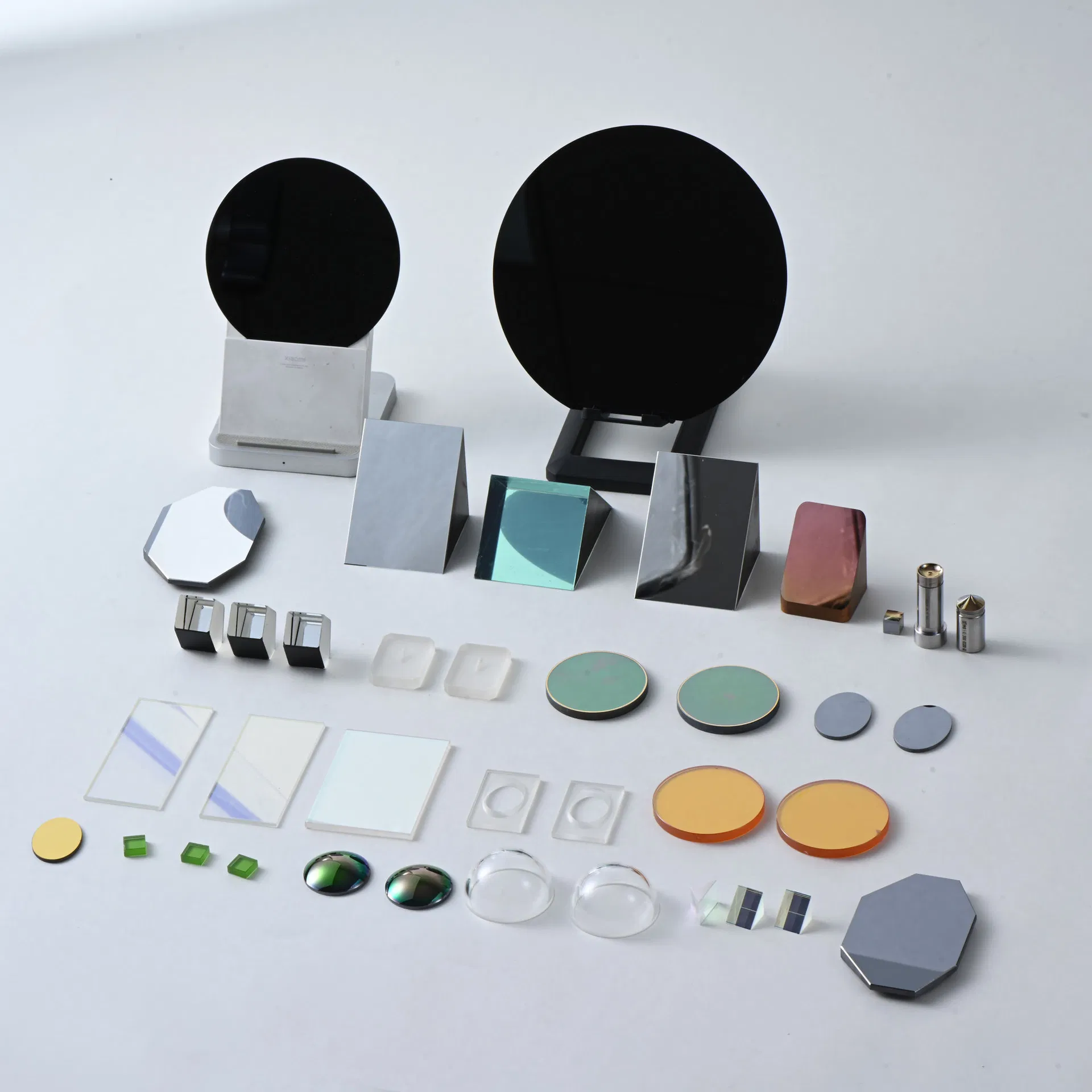
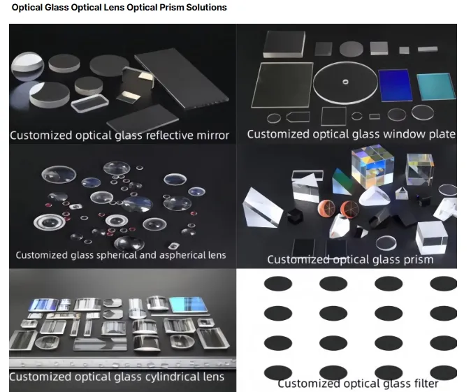
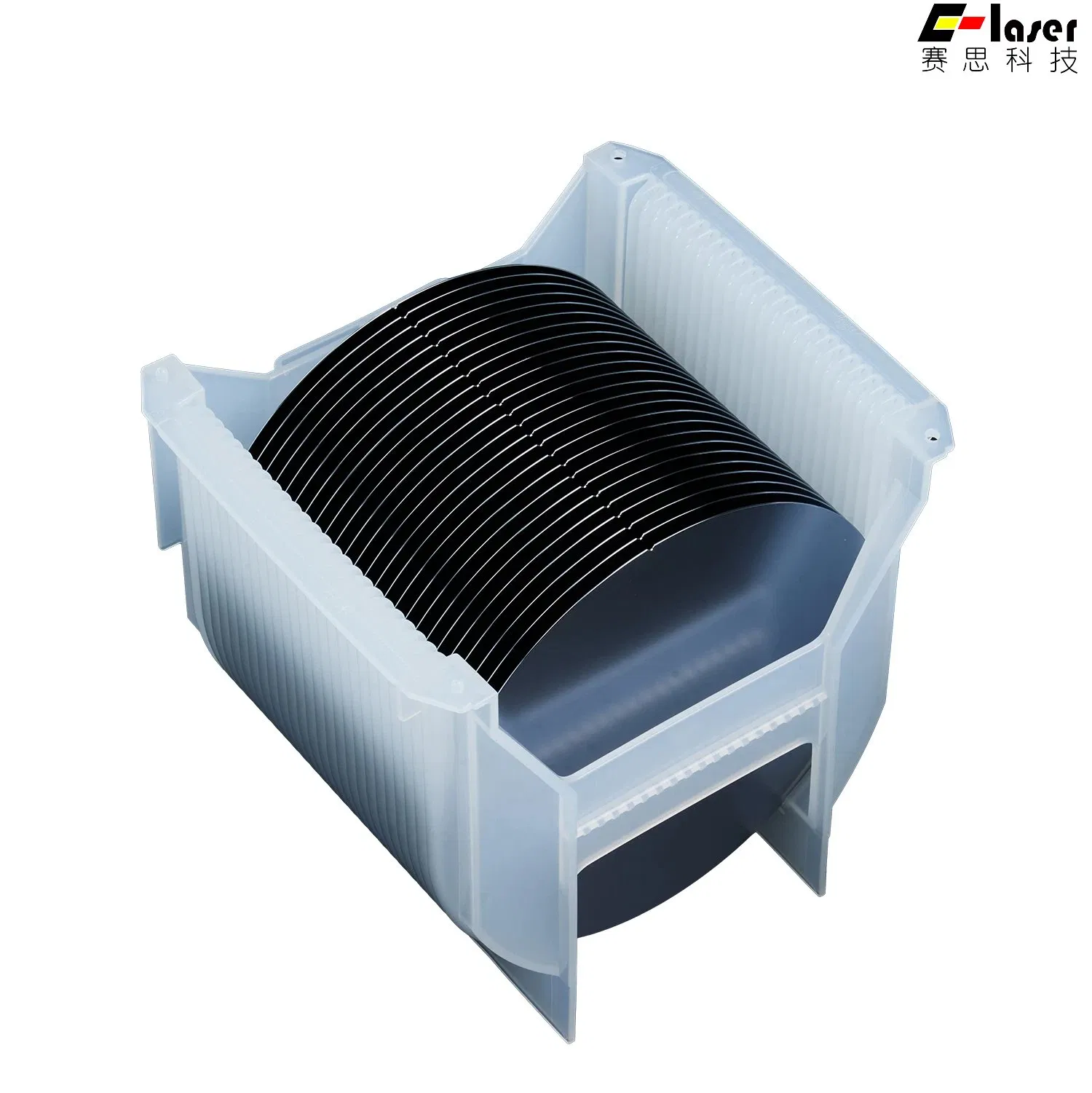
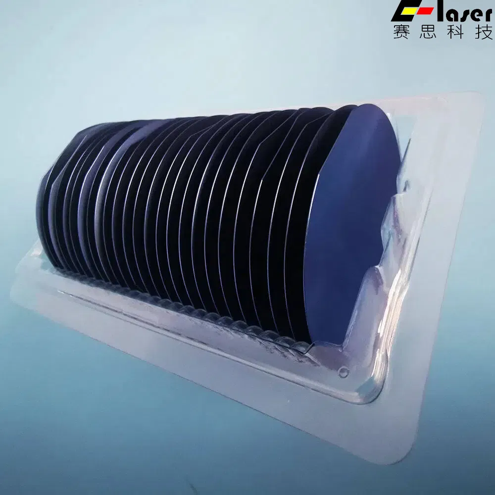
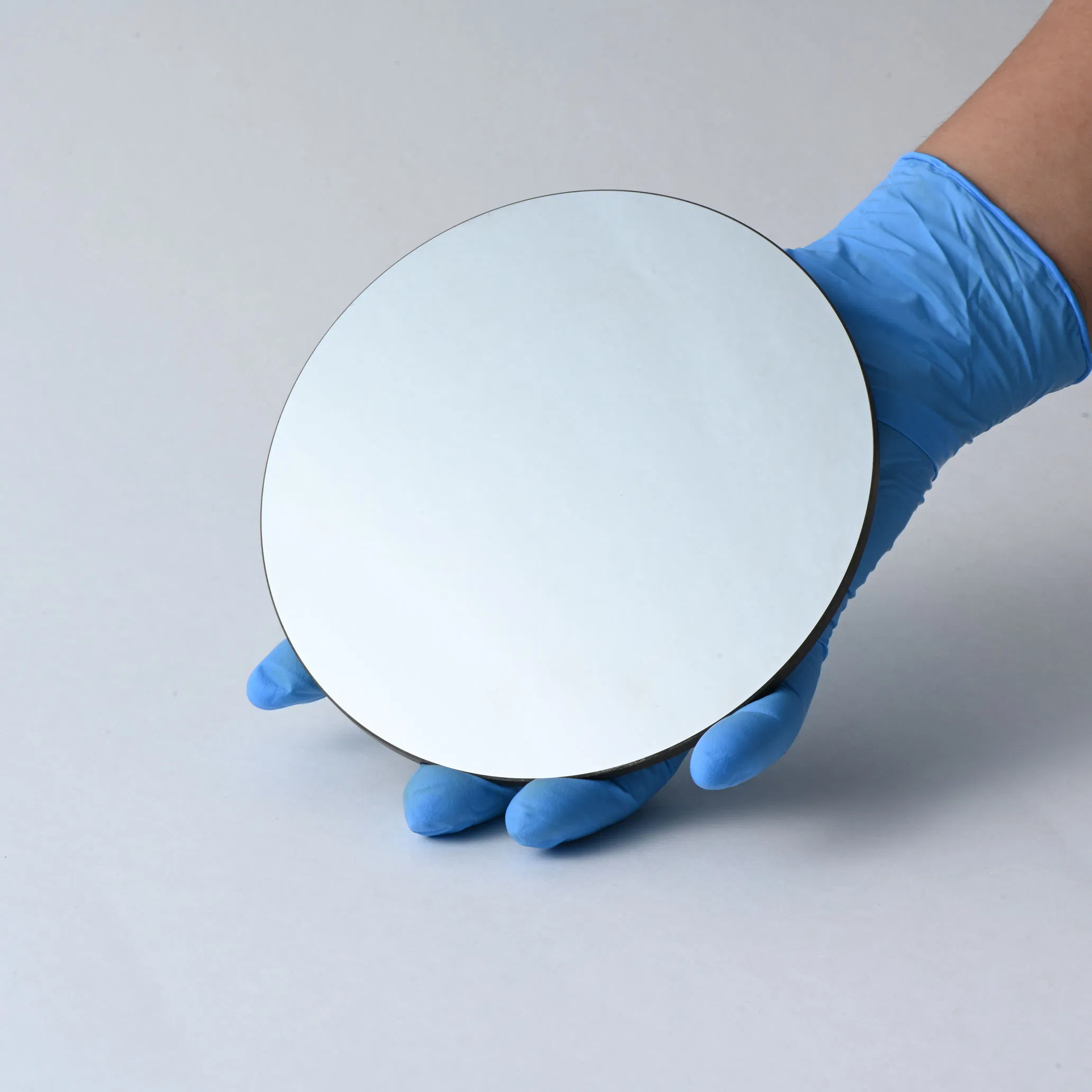
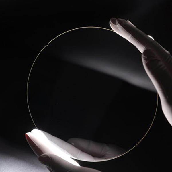
Silicon (Si) and germanium (Ge) are the most widely used infrared optical materials. They feature metallic luster, high hardness, high refractive index, and small dispersion. While opaque in the visible light band, they offer excellent transmittance in the infrared band (3 ~ 5um).

Due to its lightweight and high transmittance in middle wave infrared systems, Monocrystalline Silicon is extensively utilized for optical lenses and infrared windows in aerospace, aviation, and ground thermal imaging systems.

Technical Specifications
Technical Data Description & Value
Substrate Monocrystalline silicon
Focal Length +-2% @10.6um
Size Tolerance 0/-0.15mm
Thickness Tolerance +/-0.05mm
Optical Character 2-5um @ Tave < 1%; 5.5-14um @Tave > 85%
Parallelism Less than 1 arc min
Surface Finish 60-40 scratch-dig
Available Sizes 4" or 6"
General Introduction to Infrared Components

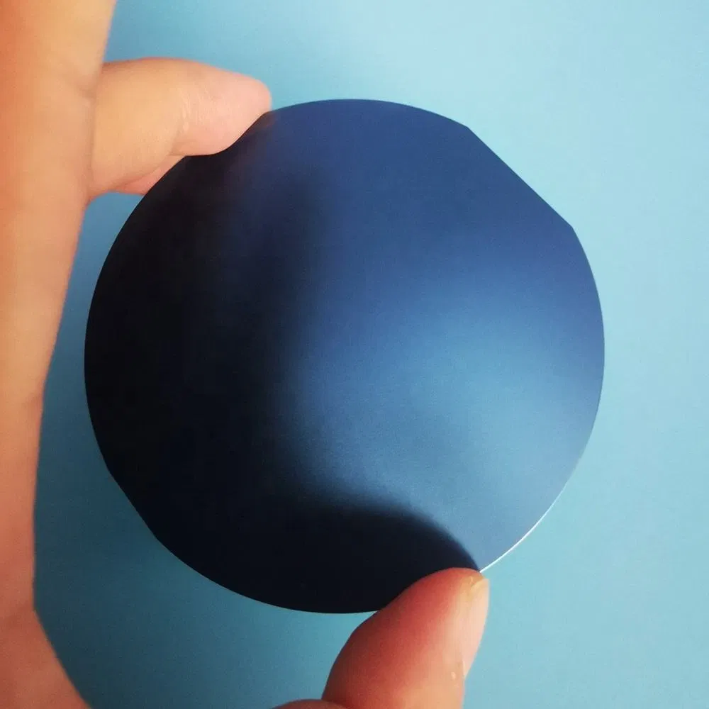
The infrared sensor filter primarily utilizes monocrystalline silicon as a substrate. Material thin films with varying refractive indices and thicknesses are alternately plated on the substrate to provide specific functions: long pass, short pass, band pass, antireflection, and reflection.

Infrared Sensor Filter Production
Related Optical Products
📍Optical Lenses: Concave, plano-convex, plano-concave, achromatic, aspheric
📍Optical Prisms: Right-angle, equilateral, Dove, Porro
📍Optical Filters: UV, IR, bandpass, neutral density, color
📍Optical Windows: Glass, sapphire, quartz (high temperature resistant)
📍Optical Mirrors: Reflective, dielectric, metal, concave, convex
Core Specifications & Advantages
Application Fields
Industrial & Scientific: Laser marking, cutting, engraving machines, microscopes, spectrometers.
Electronics & Medical: Cameras, projectors, medical imaging, optical communication.
Aerospace & Automotive: Vehicle-mounted cameras, HUD systems, satellite communications.
Frequently Asked Questions (FAQ)
1. What are the primary advantages of using Monocrystalline Silicon for IR optics?
Monocrystalline silicon offers high transmittance in the middle wave infrared band (3-5um), is lightweight, and has excellent physical properties, making it ideal for aerospace and thermal imaging systems.
2. What level of surface finish can be achieved?
Our standard surface finish is 60-40 scratch-dig, with the capability of polishing to a roughness of Ra ≤ 0.01μm to ensure minimal scattering and high precision.
3. Are custom sizes and coatings available for the silicon wafers?
Yes, we support customization for diameters ranging from 1mm to 500mm. We also offer various coating options including Anti-Reflective (AR), hydrophobic, and other specialized thin-film coatings.
4. What are the typical dimensional tolerances for these substrates?
Standard size tolerance is 0/-0.15mm, and thickness tolerance is +/-0.05mm. For high-precision requirements, we can achieve dimensional tolerances of ±0.02mm.
5. In which industries are these optical components most commonly used?
They are widely used in industrial laser equipment, scientific research instruments (microscopes/spectrometers), electronic devices, automotive HUD systems, and aerospace communication.
6. How is product quality ensured during manufacturing?
We utilize advanced CNC optical grinding and polishing machines along with professional testing instruments like interferometers and spectrophotometers to perform 100% inspection before delivery.

Related Products