High-Precision Laser Wafer Marking System for Semiconductor Manufacturing

Customization: Available
After-sales Service: Online Service
Warranty: 12 Months

Product Description

📋 Basic Information
Model NO.
HMLY-DB-005
Laser Visibility
Visible
Applicable Material
Metal
Cooling System
Air Cooling
Technical Class
Pulse Laser
Laser Wavelength
Fiber Laser
Type
Semiconductor Laser Marking
Sub-Micron Accuracy
<10μm Marks
Laser Wave
355nm
Laser Power
4W / 7W / 10W / 15W / 25W
Origin
China
Production Capacity
50000
🔍 Product Overview

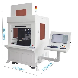
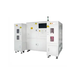
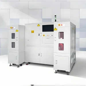
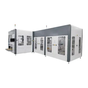
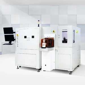
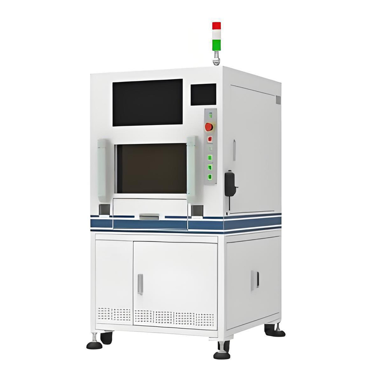
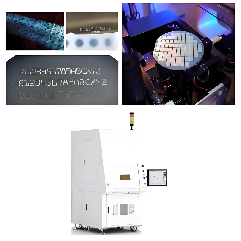
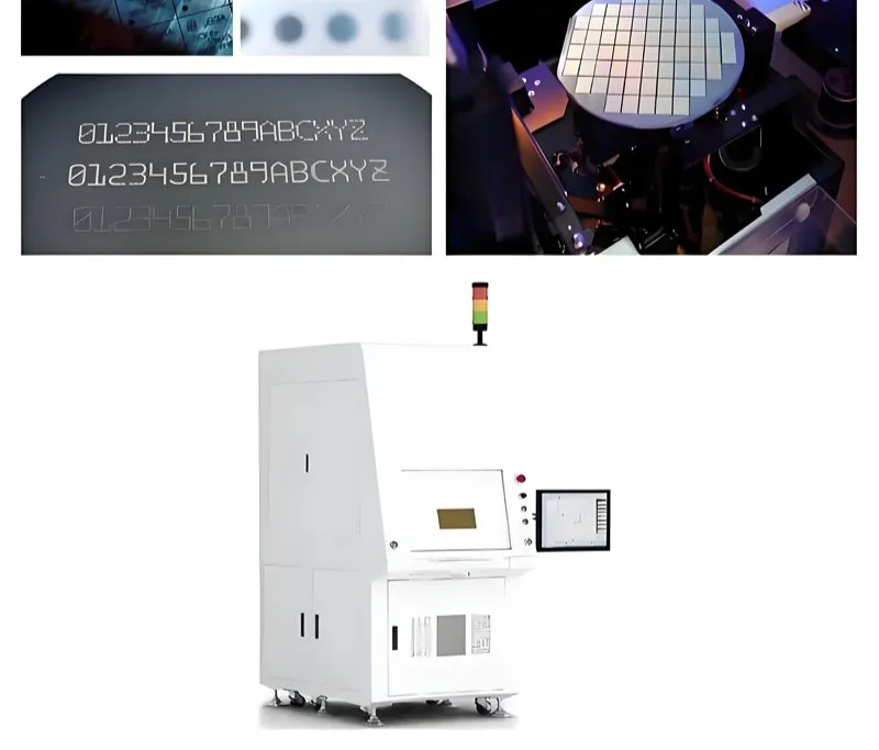
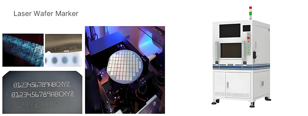
Automatic 8-12 Inches Wafer Marking Equipment with a Crystal Loading System

The Wafer Marking Machine is a high-precision, automated system designed for the laser marking of semiconductor wafers with 8-12-inch compatibility. It integrates robotic handling, automatic calibration, and advanced laser marking to ensure efficient and clean processing. The machine supports SECS/GEM communication and can be customized for various marking patterns, including barcodes (SEMI T1) and QR codes, while maintaining ISO Class 2 cleanliness in controlled environments.

Laser Wafer Marking System
Semiconductor Manufacturing Equipment
⚙️ Technical Specification
Specification Banner
Feature Details
Laser Wavelength532nm
Cooling MethodWater Cooling
Control SystemGalvanometer + Control Card (Windows 7/10)
Supported File FormatsDXF, PLT
Power SupplySingle-Phase 220V, 4KW
Optional FeaturesQR Code (DM), Custom Marking Designs
🌡️ Working Conditions

Temperature: 20-25°C (controlled environment)

Humidity: 35-60% (no condensation)

Power Supply: Single-phase 220VAC, 50Hz, 32A

Compressed Air: ≥150L/min, 0.5-0.7MPa (dehydrated & degreased)

Cooling Water: Purified water (for laser cooling)

🚀 Key Features
Feature 1
Feature 2
🎯
High-Precision Marking

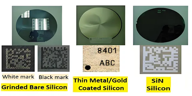
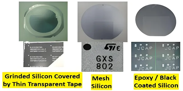
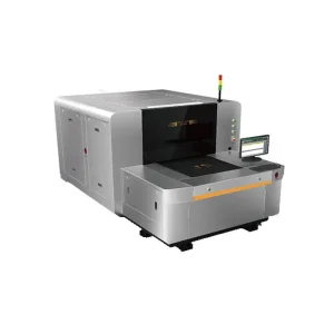
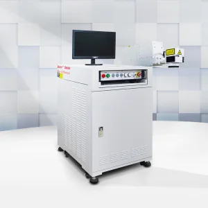
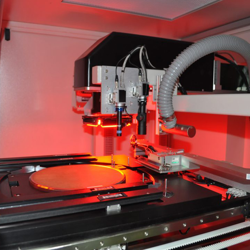
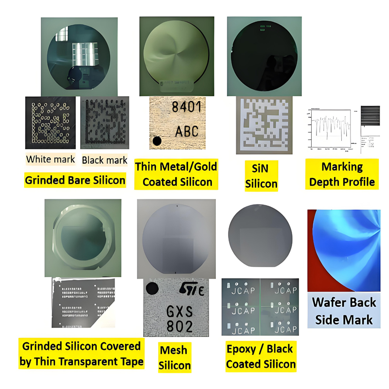
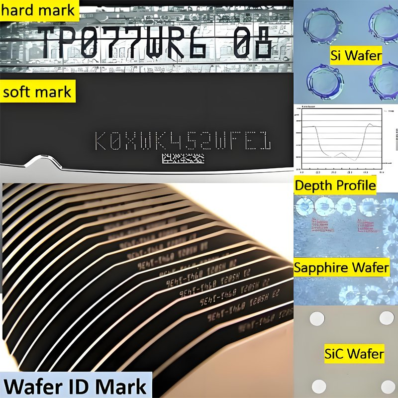
Equipped with 532nm laser (water-cooled) for clear and durable wafer markings.

🤖
Automated Handling

Dual-arm robotic system with ±0.1mm repeatability for wafer loading/unloading.

🔄
Auto-Calibration

3-second center and angle detection for accurate positioning.

🛡️
Cleanroom-Friendly

Optional FFU (H14 filter, 99.997% efficiency) and dust extraction system.

🌐 Application Areas

The Wafer Marking Machine is designed for high-precision, automated laser marking in the semiconductor and electronics manufacturing industries.

  • Semiconductor Manufacturing: Wafer Identification (UWM), 2D barcodes (SEMI T1) or QR codes.
  • LED & Optoelectronics: High-resolution marking on GaN, SiC, and sapphire wafers.
  • Solar & Photovoltaic: PV wafers for batch tracking and quality control.
  • MEMS & Advanced Packaging: Wafer-level marking for accelerometers and gyroscopes.
  • Automotive Power Electronics: Marking SiC & GaN power devices for EV inverters.
  • Medical Devices: Laser etches pacemakers and lab-on-a-chip devices.
Frequently Asked Questions
What is a Wafer Marking Machine?
It's a high-precision laser system designed to permanently mark wafers (Si, GaN, SiC, sapphire, etc.) with barcodes, QR codes, or alphanumeric IDs for traceability.
What types of lasers are used for different materials?
Fiber Lasers (1064 nm) for metals; UV Lasers (355 nm) for delicate wafers like GaN; and Green Lasers (532 nm) for glass and ceramics.
What is the marking resolution of the machine?
The system achieves a sub-micron accuracy with marking resolution up to 10 μm, ideal for miniaturized microelectronics.
Does the system support automation standards?
Yes, the machine supports SECS/GEM communication and is compatible with SEMI-standard wafer cassettes for full fab integration.
Is the equipment suitable for cleanroom environments?
Yes, it features cleanroom-friendly designs with optional H14 FFU filters maintaining 99.997% efficiency to meet ISO Class standards.
Which industries primarily use this technology?
Key industries include Semiconductor fabs, LED/Optoelectronics, Solar/PV manufacturing, MEMS packaging, and Automotive power module production.

Related Products