The landscape of Semiconductor Wafer Laser Dicing Systems in India is undergoing a seismic shift. As the Indian government pushes the "Make in India" initiative and the "Semicon India" program, the demand for high-precision manufacturing equipment has reached an all-time high. Major industrial corridors in Gujarat (Dholera), Karnataka, and Tamil Nadu are transforming into global hubs for Assembly, Testing, Marking, and Packaging (ATMP) and full-scale Wafer Fabrication.
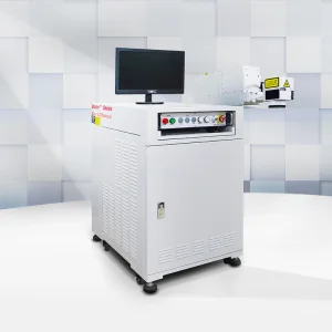
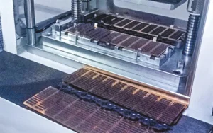
Traditional blade dicing, once the industry standard, is hitting its physical limits as wafers become thinner and materials become more exotic, such as Silicon Carbide (SiC) and Gallium Nitride (GaN). In the context of India's growing focus on Electric Vehicles (EVs) and 5G infrastructure, these materials are crucial. Laser dicing offers a non-contact process that eliminates mechanical stress, prevents chipping, and significantly increases die yield—a critical factor for the cost-sensitive Indian market.
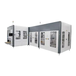
From the high-tech laboratories in Hyderabad focusing on material diffusion to the massive automotive electronics factories in Pune, the application of laser dicing and marking systems is diverse. Our systems are engineered to handle the unique environmental conditions of Indian factories, ensuring stability even in varied humidity and temperature settings through advanced PLC-controlled cleaning and cooling systems.
Over a decade of R&D in fiber laser technology specifically tuned for semiconductor substrates and advanced industrial materials.
Rigorous quality control systems and global technology integration ensure that our equipment meets international Fab standards.
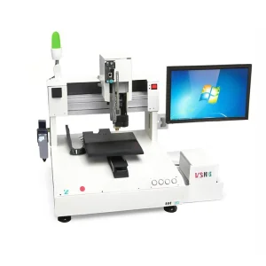
Integrating CCD vision systems and intelligent automation for high-speed, error-free production in large-scale Indian manufacturing units.
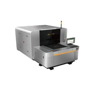
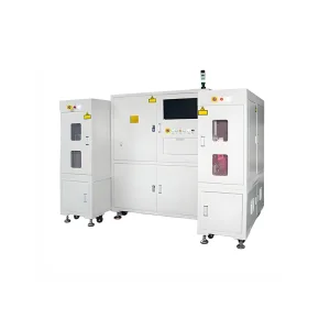
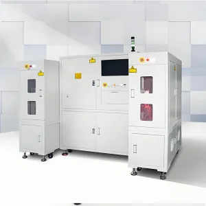
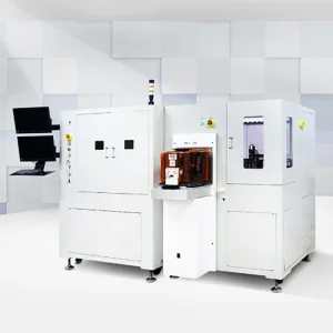
The next frontier for Semiconductor Wafer Laser Dicing Systems Manufacturers in India is the optimization of Wide Bandgap (WBG) semiconductors. SiC is becoming the backbone of India's power electronics. Our "Fully Automatic Green Laser Cutting System" is specifically designed to address the hardness of SiC, providing a clean cut with a minimal Heat Affected Zone (HAZ). This ensures that the power modules used in Indian solar inverters and EV powertrains have the highest possible reliability.
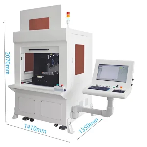
Furthermore, as India moves towards 12-inch wafer processing, our systems are already future-proofed. The "Precision Laser Wafer Marking System for 8-Inch and 12-Inch Sizes" allows Indian fabs to scale their production without needing to replace core infrastructure. This scalability is vital for the nascent Indian semiconductor industry to remain globally competitive.
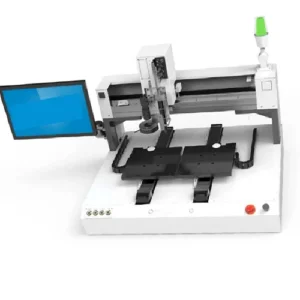
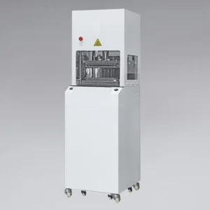
As an SEO optimizer and designer, we recognize that the first step for India is dominating the ATMP (Assembly, Testing, Marking, and Packaging) sector. Our laser marking and dispensing systems are built for this specific niche, offering high-throughput solutions that integrate seamlessly into existing production lines in Chennai and Noida. Reliability isn't just a buzzword; it's the difference between a successful fab and a costly downtime.
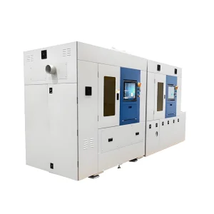
As a leading Semiconductor Wafer Laser Dicing Systems Manufacturer, our mission is to support the local ecosystem with not just machines, but complete processing solutions. We offer extensive ODM and OEM services to meet the custom requirements of Indian startups and established tech giants alike. Our commitment to E-E-A-T principles ensures that every piece of equipment—from the "High-Performance Sic Laser Annealing System" to our "Advanced Wastewater Treatment System"—is backed by verifiable engineering excellence and a global track record.
The future of semiconductor manufacturing in India is bright, and it is powered by light. Join us in building a self-reliant India through precision laser technology. Contact our technical team today to explore how we can optimize your production line for the challenges of tomorrow.