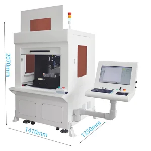
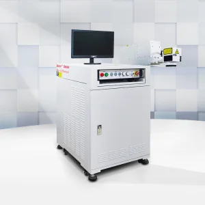
High-performance wafer processing equipment optimized for Finnish microelectronics manufacturing standards.
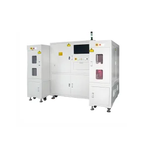
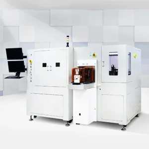
Finland has emerged as a critical node in the European semiconductor ecosystem, particularly within the specialized domains of MEMS (Micro-Electro-Mechanical Systems), power electronics, and photonics. Centered around major hubs like Espoo (Otaniemi), Oulu, and Tampere, the Finnish semiconductor industry is defined by its focus on high-value-added components. As the global demand for electric vehicles (EVs) and 5G/6G infrastructure surges, Finnish manufacturers are increasingly adopting Semiconductor Wafer Laser Dicing Systems to replace traditional mechanical sawing methods.
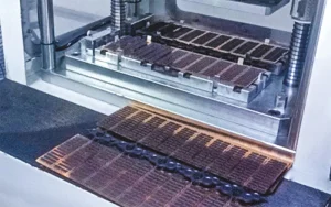
The Finnish industrial strategy, supported by the EU Chips Act, emphasizes domestic capabilities in wafer fabrication. Companies operating in Finland, such as those collaborating with the VTT Technical Research Centre of Finland, require extreme precision when dicing brittle materials like Silicon Carbide (SiC) and Gallium Nitride (GaN). Our laser dicing solutions provide the required accuracy to handle the thin, fragile wafers used in Oulu's world-leading telecommunications research and Espoo's quantum computing startups.
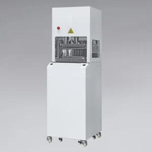
Focusing laser energy inside the wafer substrate creates a modified layer without damaging the surface. This is essential for the ultra-thin wafers used in Finnish IoT devices.
Our Green Laser systems provide superior absorption rates for SiC wafers, significantly reducing the Heat Affected Zone (HAZ) and increasing die yield per wafer.
Utilizing high-speed CCD vision for real-time alignment ensures that even warped wafers are diced with sub-micron accuracy, matching Finland's Industry 4.0 requirements.
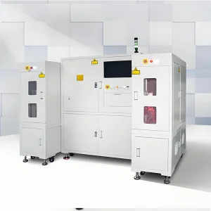
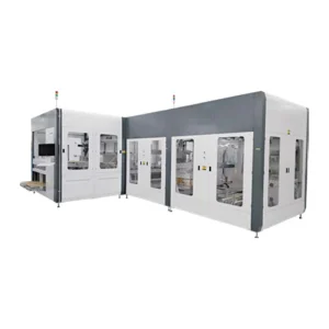
In the harsh industrial environments of Northern Europe, reliability is non-negotiable. Foshan Stylo Laser Co., Ltd. integrates German-engineered laser sources with proprietary CNC control software to ensure 24/7 operation. Whether it is for the automotive sensors produced in the Helsinki region or high-frequency filters for 5G base stations, our systems are designed to minimize material waste and maximize throughput.
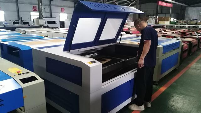
Foshan Stylo Laser Co., Ltd. is a professional manufacturer specializing in advanced industrial laser processing equipment. We are dedicated to delivering high-precision, high-efficiency laser solutions for modern manufacturing industries that require superior accuracy and stable performance.
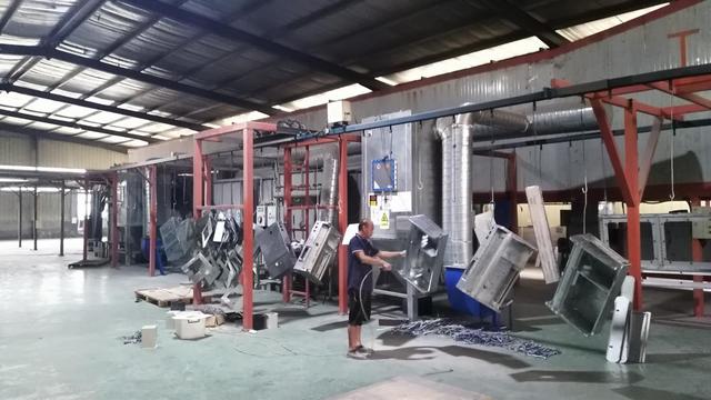
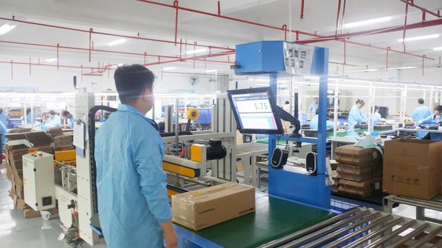
Our core technology is applied in the processing of ceramic materials, electrical steel, and advanced industrial materials used in transformers, electronics, and energy systems. By integrating fiber laser technology, CNC control systems, and intelligent automation, we provide cutting solutions that improve production efficiency while maintaining exceptional quality.
Learn More About Our Expertise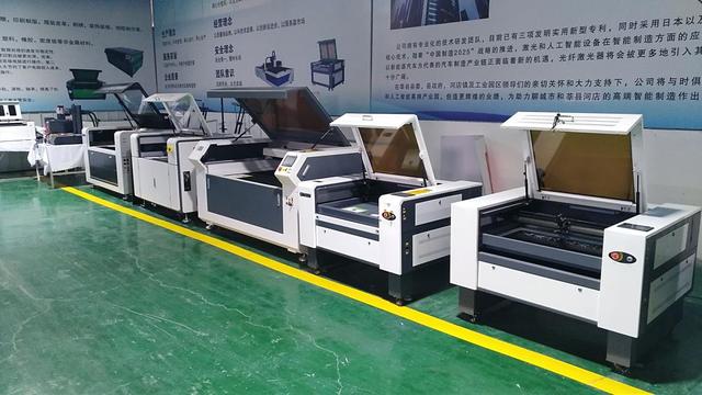
Our semiconductor wafer laser dicing systems are specifically adapted for several key Finnish industries:
Comprehensive portfolio for high-tech manufacturing, from IC marking to wastewater crystallization.
Choosing a supplier for semiconductor wafer laser dicing systems in Finland requires a partner who understands both the technical rigor of microelectronics and the logistical needs of the Northern European market. Our systems are built to meet CE standards and are compatible with the cleanroom requirements (ISO 14644-1) typical of Finnish fab facilities.
We provide full technical support, from initial wafer testing to on-site installation and calibration. Our expertise in Sic laser annealing and wastewater treatment systems further demonstrates our commitment to a holistic, sustainable manufacturing approach, aligning with Finland's green transition goals.
Contact our engineering team today for a customized consultation on how our laser solutions can optimize your production in Finland.
Get a Professional Quote Today