As the largest economy in Southeast Asia, Indonesia is undergoing a profound digital transformation. Under the government's "Making Indonesia 4.0" initiative, the electronics and semiconductor industries have been prioritized as key drivers of national economic growth. This shift from simple consumer electronics assembly to sophisticated semiconductor fabrication and packaging has created an unprecedented demand for Semiconductor Wafer Laser Dicing Systems.
Batam, with its Special Economic Zone status and proximity to Singapore, has become a hub for microelectronics. Meanwhile, industrial corridors like Cikarang and Karawang are attracting global Tier-1 automotive and tech suppliers. These regions require localized suppliers and exporters of high-precision laser equipment to maintain competitive edge in the global supply chain.
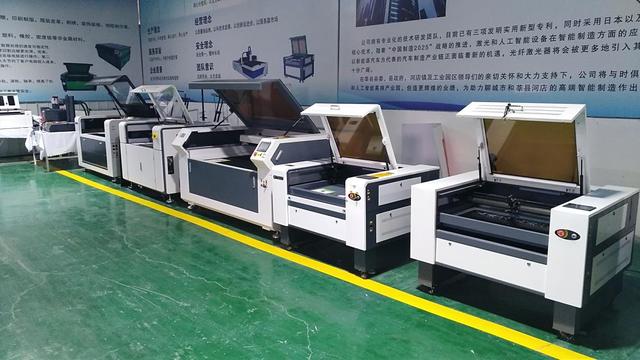
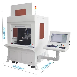
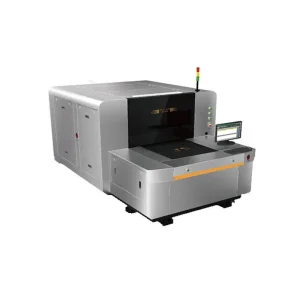
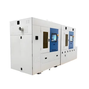
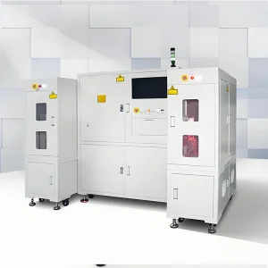
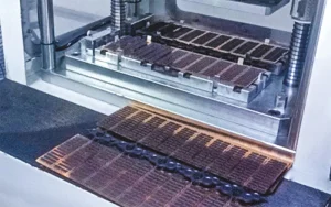
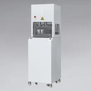
Traditional blade dicing is increasingly reaching its physical limits, especially as wafers become thinner and materials like Silicon Carbide (SiC) and Gallium Nitride (GaN) become standard for electric vehicles (EVs) and 5G equipment. Our laser dicing systems offer:
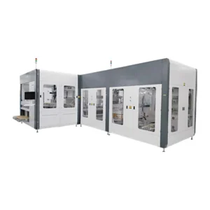
Our equipment is engineered to address the specific environmental and industrial challenges found in Indonesia:
Precision Accuracy
Production Stability
Efficiency Gain
With Indonesia positioning itself as a global player in the EV battery supply chain, the demand for power semiconductors is soaring. Our Fully Automatic Green Laser Cutting Systems are ideal for dicing SiC wafers used in EV inverters and charging stations.
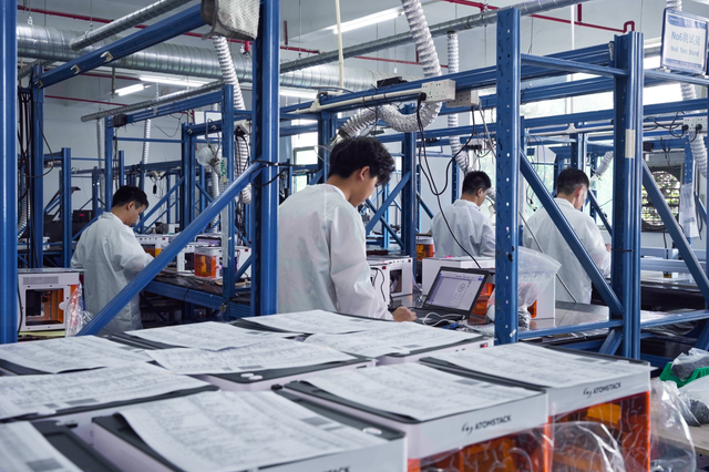
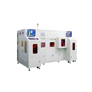
The burgeoning Indonesian middle class and the rapid adoption of IoT devices require high-volume production of ICs and MEMS sensors. Our high-speed IC marking and dicing systems ensure that local manufacturers can meet domestic demand without relying on expensive imported finished goods.
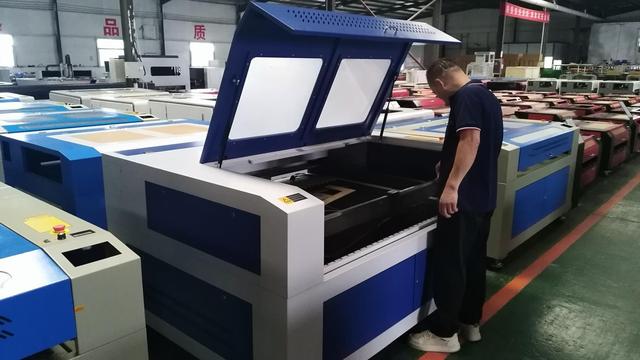
At Foshan Stylo Laser Co., Ltd., we don't just supply machines; we provide expertise. Our engineering team brings decades of experience in laser-material interaction. For the Indonesian market, we offer comprehensive technical consulting, ensuring that the laser parameters are perfectly tuned for the specific humidity and climate conditions of the region, which can often affect precision optics if not properly managed.
We understand that downtime in a semiconductor line is catastrophic. Our export model for Indonesia includes robust remote diagnostics, rapid spare parts fulfillment, and local technical training for engineers in Jakarta and Batam.
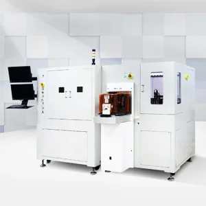
The future of semiconductor dicing in Indonesia lies in AI-driven defect detection. Our newest systems integrate CCD vision systems with machine learning algorithms that can detect wafer flaws in real-time during the dicing process. This reduces waste and ensures that only 100% compliant dies proceed to the packaging stage.
Furthermore, as Indonesia moves toward more sustainable manufacturing, our fiber-laser based systems offer a significant reduction in energy consumption compared to older CO2 or mechanical systems, aligning with the Green Industry standards set by the Indonesian Ministry of Industry.